Development of atomic spalling technology that precisely controlled the crack propagation depth in the sub-nanometer range |
Because of their superb electrical, optical, and thermal properties, transition metal dichalcogenides (TMDCs) have been considered a strong contender to replace Si for next-generation semiconductor devices. A primary requirement for industrialization is to develop a controlled manufacturing technique that can both obtain electronic-grade TMDCs over a large-scale dimension and allow facile tuning of their electrical properties. Among the various synthetic approaches, the mechanical cleavage method is known as the only way to obtain electronic-grade TMDCs. However, since it was not able to control the size, yield, and a number of layers of TMDCs, it has been considered an unfavorable method in terms of mass production until now.
Korean researchers at Ajou University reported a high-quality and high-throughput TMDCs manufacturing technique that not only guarantees large-size but also provides control of a number of TMDCs layers. This study was published in the Matter in August 2022.
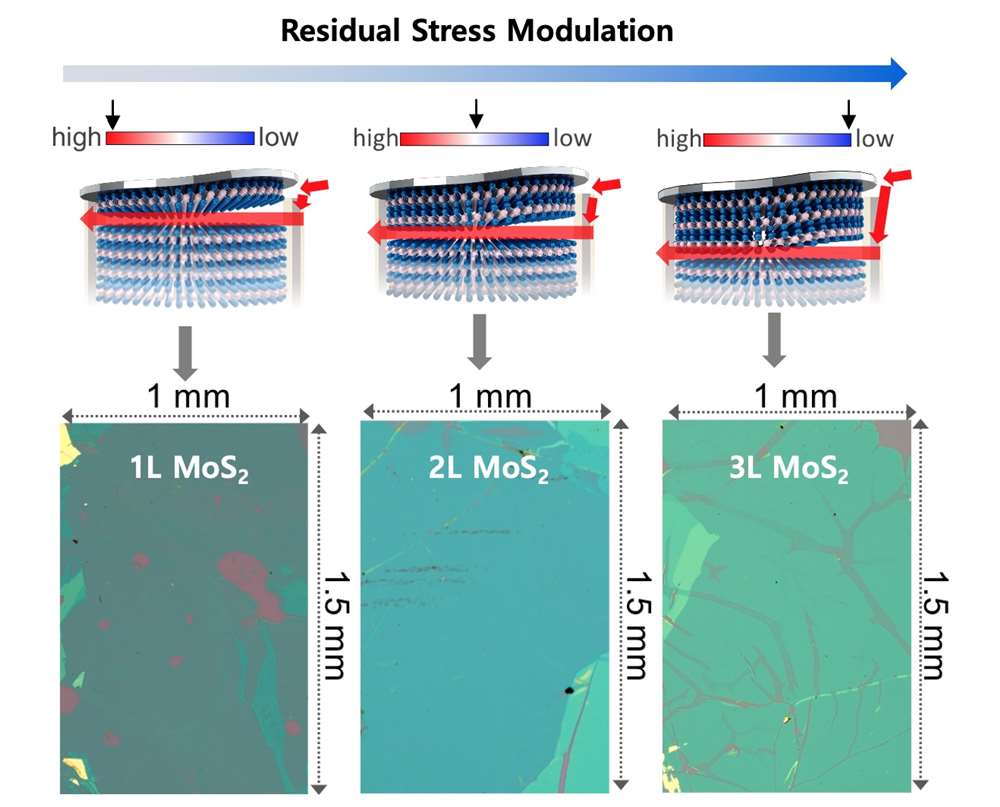
The researchers discovered that being a layered crystal with a weak interlayer vdW force enables to control of the crack propagation depth at the scale corresponding to the single atomic thickness by adjusting the internal stress of the stressor film. Consequently, the researchers achieved large-area, high-quality TMDCs (MoS2, MoSe2, and WSe2) with a controlled number of layers via an atomic spalling approach. Moreover, the researchers fabricated a large-area vdW heterostructure based on a combination of spalled MoS2 and spalled monolayer graphene and demonstrated 6 x 6 matrix photodetector arrays, which have only been implemented with large-area synthesized materials, so far.
Prof. Lee said that “The atomic spalling technology will provide a way to capture quality and productivity, which is regarded as the biggest obstacle in the use of 2D semiconductor materials” and “Our finding will play an important role in diagnosing/solving the root cause of the film exfoliation problem occurring in electronic devices manufactured with multi-layered structure.
|
(Up) Schematic of the atomic spalling process. By modulating the residual stress of stressor film, spalling depth was determined with monolayer, bilayer, and trilayer spalled MoS2, (Down) OM images of the monolayer, bilayer, and trilayer spalled MoS2 |
[Reference] Moon J.-Y. et al., (2022) “Layer-engineered atomic-scale spalling of 2D van der Waals crystals” Matter
DOI: https://doi.org/10.1016/j.matt.2022.07.021
[Main Author] Ji-Yun Moon (1st Author, Ajou University), Jae-Hyun Lee (Ajou University) Seok-Kyun Son (Mokpo National University)
* Contact : Prof. Jae-Hyun Lee (jaehyunlee@ajou.ac.kr)