High-Performance, Low-Power Electronics Enabled by Two-Dimensional Material Inks |
As the silicon-based electronics are reaching the physical limit, two-dimensional (2D) materials have emerged as a promising class of electronic materials for the era of Industry 4.0. However, their application in semiconductor industry has been impeded by the lack of a cost-effective method to produce 2D material films uniformly over wafer-scale areas. Korean researchers at Sungkyunkwan University (SKKU) has developed new 2D material inks for high-performance, low-power electronic devices. This study was published in the online edition of "Advanced Materials" in December 2021.
Since the demonstration of prototype field-effect transistors based on microscale semiconducting 2D flakes, extensive research has focused on wafer-scale production of 2D material films for practical applications. Chemical vapor deposition (CVD) has been widely investigated to grow 2D materials over large areas, but the economic feasibility is not met because of the high processing temperature and limited throughput. Alternatively, liquid-phase exfoliation of 2D layered crystals using ultrasonication has shown promise to mass produce 2D materials at low cost. However, the resulting 2D nanosheets exhibit a broad distribution in thickness and small lateral size, which hinders the formation of uniform, continous films when the dispersion is coated on a substrate.
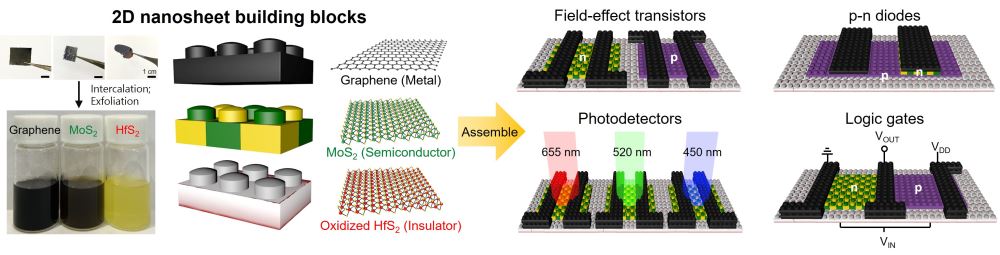
To overcome this issue, the research group led by Prof. Joohoon Kang inserted organic intercalants (2 nm in diameter) in between individual 2D layers of the crystal via electrochemical reaction and then applied a mild sonication to exfoliate the nanosheets. Because the dispersion consists of nanosheets with a narrow thickness distribution and large lateral sizes, wafer-scale, continuous thin films could form after simple solution coating processes. By assembling metallic, semiconducting, and insulating nanosheets into building blocks, the researchers demonstrated various electronic devices that outperform previous solution-processed 2D material devices at much lower operating voltages. “We believe that our work opens prospects for scalable fabrication of high-performance 2D material electronics and optoelectronics because our strategy is generally applicable to a broad library of layered crystals,” Prof. Kang said.
|
2D material inks from electrochemically driven molecular intercalation and their assembly into diverse functional electronics and optoelectronic devices. |
[Reference] Kim, J et al., “All Solution-Processed van der Waals Heterostructures for Wafer-Scale Electronics.” Advanced Materials 2021, accepted, DOI: 10.1002/adma.202106110
[Main Author] Jihyun Kim (Sungkyunkwan University), Dongjoon Rhee (Sungkyunkwan University), Okin Song (Sungkyunkwan University), Joohoon Kang (Sungkyunkwan University)
* Contact : Professor Joohoon Kang (joohoon@skku.edu)